
Our work spans multiple directions across photonics and atomic quantum systems.
Scalable trapped-ion quantum systems
Trapped ions constitute a leading approach to large-scale quantum information processing (QIP), as well as precision metrology. The qubits, based on individual atoms in the void, are pristine and well understood; major bottlenecks to scaling lie in the classical control apparatus required to interface to these qubits, and importantly in the optics used to deliver and collect the photons with which qubits are controlled and measured. Our group is pursuing an integrated architecture for ion qubit control, utilizing nanophotonic waveguide devices co-designed and integrated with ion trap devices. These approaches stand to enable control of large-scale atomic quantum systems, while simultaneously reducing noise sources and infidelities associated with conventional implementations — and thus attack key problems in extending quantum information systems to meaningful scales.
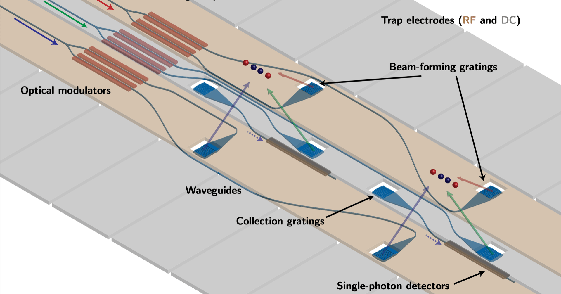
Schematic of integrated architecture for optical control/readout of trapped-ion quantum systems. From arXiv:2102.03323 (2021); see also Nat. Nano. 11, 1066-1070 (2016) and K.Mehta, Ph.D. Thesis, MIT (2017).
Novel atom-light interactions
The use of integrated optics for control of atomic systems brings possibility for interactions between individual atoms and photons that may be challenging or impossible to achieve with conventional free-space optics. This results from the ability to tailor guided and resonant mode structures on wavelength scales, and the high passive phase stability of integrated photonic beampaths.
We are exploring the potential and limits of such techniques to enable new functionality for quantum logic, laser cooling, and quantum state manipulation/measurement. This work leverages electromagnetic design and optimization in close conjunction with atomic physics, with relevance both to quantum information processing and precision metrology.
Photonic materials and devices
The vast majority of integrated photonics research to date has focused on telecommunications wavelengths, with great impact in silicon photonics and classical communications. The visible and blue/UV wavelength ranges of interest to many atomic species are challenging to access with conventional photonic materials, particularly with respect to active devices (acousto- and electro-optic modulators, e.g.). Future scaling of trapped-ion, atomic, and color center-based quantum technologies will hinge critically on innovations in photonics in these wavelength regimes. We are introducing and studying new materials platforms and device architectures for integrated optics at these wavelengths. We’re interested in device and material characteristics both at room temperature and in cryogenic environments, and in leveraging modern nanofabrication techniques to explore the limits of active acousto- and electro-optical control at short wavelengths. Applications extend beyond quantum systems to, e.g. biochemical sensing and spectroscopy, and visible wavelength communications.